Voltage Controlled Volume circuit
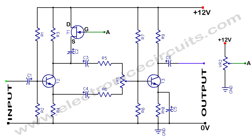
This voltage controlled volume control circuit offers an unusual approach to the well-known problem of distortion in active-device attenuators. The zero-output in this case is obtained by allowing equal signals of opposite phase to cancel each other.

| PARTS LIST | |
| R1 | 82kΩ |
| R2 | 33kΩ |
| R3 | 2.2kΩ |
| R4 | 2.2kΩ |
| R5 | 56kΩ |
| R6 | 56kΩ |
| R7 | 220kΩ |
| R8 | 100kΩ |
| R9 | 2.7kΩ |
| R10 | 1kΩ |
| VR1 | 1kΩ |
| VR2 | 470kΩ |
| C1 | 1µF 16V |
| C2 | 100µF 16V |
| C3 | 4.7µF 16V |
| C4 | 4.7µF 16V |
| C5 | 47µF 16V |
| C6 | 4.7µF 16V |
| T1 | BF245 |
| T2 | BC109 |
| T3 | BC109 |
The input transistor operates as a ‘concertina’ phase-splitter, producing equal-amplitude opposite-phase voltages at its collector and emitter. The two signals can be brought into complete cancellation, at the summing point, by means of preset p1. The harmonic content of the two signals is very small, but not quite identical.
There will therefore actually be an even smaller distortion output at the nominally ‘zero’ point.
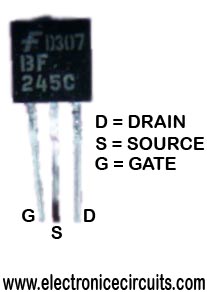
If something now happens to the amplitude ratio of the signals at the summing point, there will be output passed to the buffer-stage. The necessary unbalance is achieved by means of the JFET and capacitor C2. The gate bias on the FET is set by the DC control voltage applied to point A. With this voltage close to zero the FET will be cut off, so that the above mentioned cancellation takes place. As this voltage is increased there will come a point at which the channel starts to ‘bleed off’ AC collector current from the splitter; this will upset the balance and so cause an output signal to appear. The more conductive the FET, The more output. Unfortunately, the more channel current there flows the lower will be negative gate bias and so the greater will be the distortion of the ‘regulated’ summing component.

The trick is now to employ only a moderate degree of unbalance – so that the FET operates at low distortion percentages. The process is helped also by the always present ‘clean’ summing component. The buffer stage provides gain, so that a sufficient output level is obtained. The Circuit’s frequency response extends from 50Hz to 35kHz (-3dB points). The input voltage should be limited to 100mV p-p: the output can be varied from ‘0’ to 1V p-p (by using the appropriate range for the control voltage at A).
Please send your ideas, which are very important for our success…
nice post. thanks.
great post as usual!
ок ладно
ок это да
ок важно
Thank you very much for writing this excellent content! I am looking forward to checking out more!
Thank you so much for posting this great content! I am looking forward to checking out more.