3.INVERTING AC AMPLIFIER

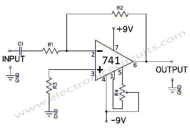
Fig.6. General Purpose Inverting AC Amplifier
| PARTS LIST | |
| R1 | 33KΩ |
| R2 | 1MΩ |
| R3 | 10KΩ |
| R4 | 10KΩ |
| C1 | 0.1µF |
Fig.6 shows a general purpose inverting type of ac amplifier.
| INPUT Z | =R1 |
| 33KΩ | |
| GAIN | =R2/R1 |
| 30 | |
| BANDWIDTH | 50Hz to 30KHz |
As the input signal is applied to the inverting input terminal, the output signal is phase inverted. The amplifier gain is decided by the ratio of the feedback components R1 and R2. The low-frequency roll-off is decided by C1 becomes equal to R1. For direct coupling to the next stage, the standing dc can be set exactly to zero by R4. For ac coupling via a capacitor, R4 can be omitted.
4. NON-INVERTING AC AMPLIFIER

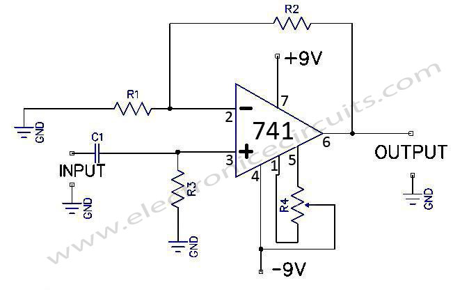
Fig.7. General Purpose Non-inverting AC Amplifier.
| PARTS LIST | |
| R1 | 10KΩ |
| R2 | 330KΩ |
| R3 | 100KΩ |
| R4 | 10KΩ |
| C1 | 0.1µF |
A general purpose non-inverting type of ac amplifier is shown in Fig.7.
| INPUT Z | =100K |
| GAIN | 1+(R2/R1) |
| 34 | |
| BANDWIDTH | 15Hz to 30KHz |
The input signal is applied to the plus input of 741 and the output therefore, has the same phase as that of the input signal. Amplifier gain can be set to any value by choosing R1 and R2 but, the higher the gain, the lower will be bandwidth of the amplifier. R3 provides a dc ground path to the bias current. The gain falls by 3 dB at a frequency where reactance of C1 equals R3. R4 may be omitted if the amplifier output is to be coupled to the next stage through a capacitor.
5. DC VOLTAGE FOLLOWER

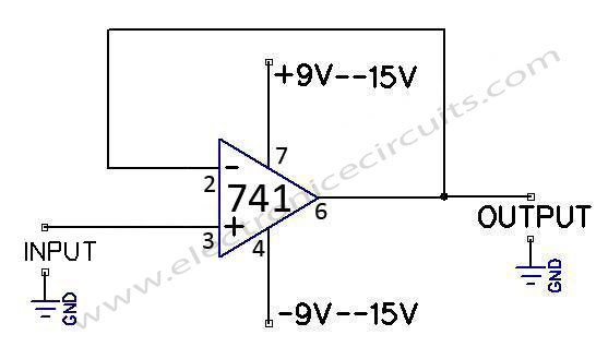
Fig.8. Unity Gain DC Voltage Follower
| INPUT Z | =VERY HIGH |
| OUTPUT Z | <1 OHMS |
| GAIN | =1 |
| BANDWIDTH | =1MHz |
A Direct coupled unity gain voltage follower is shown in Fig.8. The circuit is useful for impedance transformation. Because of hundred per cent negative feedback., the input impedance is very high, and the output impedance is very low. The frequency response extends up to 1 MHz. The signal input source must provide a direct path to ground of less than 100k ohms for input bias current. The circuit can deliver load current up to 10 milliamperes.
6. AC VOLTAGE FOLLOWER

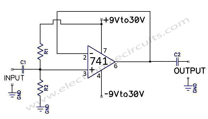
Fig.9. AC Coupled Voltage Follower.
| PARTS LIST | |
| R1 | 1MΩ |
| R2 | 1MΩ |
| C1 | 0.1µF |
| C2 | 0.47µF |
An ac coupled unity gain voltage follower operating on a single supply is shown in Fig.9. Voltage divider network of R1 and R2 provides a dc voltage equal to half the supply voltage to the non-inverting input of the 741. The output dc voltage therefore stands at half the supply voltage. The output signal swings above and below this value. The standing dc voltage at pin 6 does not matter because the output is coupled to the next stage via a capacitor.
The input impedance is equal to the value of R1 and R2 in parallel, i.e. 500k ohms in this case. Because of hundred per cent negative feedback, the output impedance is very low. For low frequency applications C1 and C2 can be replaced by electrolytic capacitors of large values.
Please send your ideas, which are very important for our success…
I am always excited to visit this blog in the evenings.Please churning hold the contents. It is very entertaining.
WONDERFUL Post.thanks for share..more wait .. ;)…
Your place is valueble for me. Thanks!…
Super informative article, thanks a million.
These designs are really cool. I like this post Keep it up dude 🙂
Thank’s for your information abaut op amp 741 – 14 pin.
INTERESTING’
minta data ic yang 8 pin
Hello. I like electronics too.