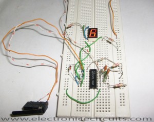
Electronic Coin Toss Circuit Diagram
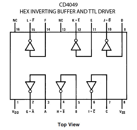
This is electronic coin toss circuit using one CD4049 IC (Hex inverting buffer and TTL driver). This IC has six buffers and it can use independently. The buffers use as simple inverters, as voltage translators, or as current drivers for interfacing TTL or other logic.
| PARTS LIST | |
| R1 | 2.7KΩ |
| R2 | 2.7KΩ |
| R3 | 15KΩ |
| R4 | 220Ω |
| R5 | 220Ω |
| C1 | 0.01µF (103) |
| C2 | 0.01µF (103) |
| D1 | 1N4148 |
| IC1, IC2, IC3, IC4, IC5, IC6 | CD4049 |
| PB1 | Push to on switch |
| DISPLAY 1 | common cathode 7-segment display |
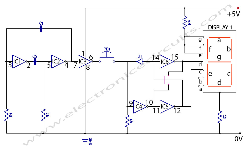
The gate IC1 and IC2 of the IC and resistor – condenser network from a relaxation oscillator. Gate IC3 of the IC is a buffer which isolates the oscillator from the load. Gates IC5 and IC6 use as a flip-flop. The LEDs will glow (either head or tail) when the corresponding gate’s output is high. The output of flip-flop will change states only when the input applied are compliment logic levels, example: high and low.For this gate IC4 is used.
Press the switch PB1 and release it. The LED will show for chance.
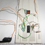
You can use a 7-segment common cathode display instead of LEDs to know the chance by reading the letters h and t.
Please send your ideas, which are very important for our success…
i resembling it Electronic plug Toss Circuit Diagram after this im your rss reader
nice